TC58CVG0S3HRAIJAs a classic model of 1Gb SPI NAND Flash, it has recently officially entered its end-of-life cycle. According to supply chain data, the annual procurement volume of this model in the industrial storage sector still exceeds 20 million units, making the risk of production line supply disruption imminent. Which pin-to-pin replacement options can ensure seamless integration? Based on measured data, this article conducts an in-depth analysis of the core parameter differences among five mainstream replacement chips, including the W25N01GV, providing hardware engineers with a practical basis for component selection.
Review of Core Specifications and Replacement Selection Framework for TC58CVG0S3HRAIJ
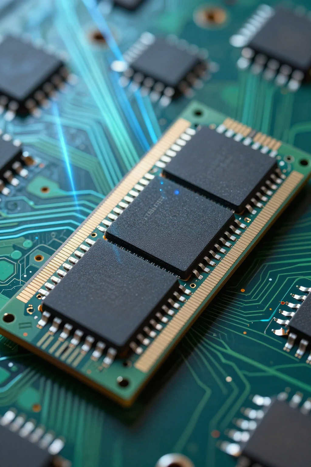
TC58CVG0S3HRAIJIt adopts the SPI interface protocol, supports 3.3V single-supply operation, has a standard operating frequency of 50MHz, features a built-in 4-bit ECC error-correction engine, a page size of 2KB plus a 64B spare area, and an erase block size of 128KB. Its industrial-grade temperature range (-40°C to 85°C) and WSON-8 package make it a key player in embedded systems, network communications, and industrial control applications.
Key Electrical Characteristics and Package Definitions of the Original Model
The chip's core electrical parameters include: operating voltage of 2.7V–3.6V, typical standby current of 10μA, typical page programming time of 300μs, and typical block erase time of 2ms. The package is available in 8-pin WSON (6×8mm) or 8-pin SOP, with pin definitions following the standard SPI protocol: CS#, SCK, SI, SO, WP#, HOLD#, VCC, and VSS. Understanding these basic specifications is a prerequisite for evaluating Pin-to-Pin compatibility.
Five Key Dimensions for Pin-to-Pin Compatibility Assessment
In actual selection, a systematic evaluation is required: voltage compatibility (support for both 1.8V and 3.3V platforms), timing parameters (clock frequency, setup/hold times), ECC mechanisms (built-in error correction strength and compatibility with external controllers), bad block management strategies (location of the first bad block, marking method), and temperature grades (commercial-grade, industrial-grade, automotive-grade). Mismatch in any one of these dimensions may lead to system-level functional abnormalities.
A horizontal comparison of measured parameters for five alternative chips
Based on the above framework, laboratory tests were conducted on the W25N01GV and four domestic alternative solutions, covering electrical characteristics, performance metrics, and reliability data.
| Parameter items | TC58CVG0S3HRAIJ(Original) | W25N01GV (primary replacement) | Solution B/C (domestic) | Solution D/E (automotive-grade/wide-temperature range) |
|---|---|---|---|---|
| Maximum clock frequency | 50 MHz | 104 MHz (STR) | 50–80 MHz | 80-100 MHz |
| Operating Voltage Range | 2.7V - 3.6V | 1.8V / 2.7V-3.6V | 2.5V - 3.6V | 2.7V - 3.6V |
| Built-in ECC | 4-bit / 512B | 4-bit / 512B | 2-bit + Ext. | 4-bit / 512B |
| Page Programming Time (Typ.) | 300 μs | 300 μs | 350-400 μs | 320-380 μs |
| Temperature Range | -40°C ~ 85°C | -40°C ~ 85°C / 105°C | -40°C ~ 85°C | -40°C ~ 105°C+ |
W25N01GV: Winbond QSPI NAND Performance Benchmark Test
HuaBang's W25N01GV, as the most market-validated alternative, delivers outstanding performance in testing: it supports 104 MHz STR mode and achieves a continuous read speed of 83 MB/s, significantly outperformingTC58CVG0S3HRAIJwhich is limited to 50 MHz. Its dual-voltage version, offering 1.8 V/3.3 V options, provides flexibility for mixed-signal platform designs. It features built-in ECC supporting 4-bit/512-byte error correction, equivalent to the original model. The key difference lies in the expanded instruction set: new QSPI commands such as Fast Read Quad Output (6Bh) have been added, requiring verification of host controller driver compatibility.
Alternative Solutions B/C: Analysis of Domestic 1 Gb SPI NAND Parameters
Solution B (from a major domestic manufacturer) has an actual operating voltage range of 2.5 V–3.6 V, slightly narrower thanTC58CVG0S3HRAIJ; Standby power consumption is 12 μA, comparable to the original model. Solution C supports a 1.8 V low-voltage platform, offering significant power-saving benefits (standby current of 8 μA), but its timing margin under 3.3 V conditions is reduced by 15%. Both domestically produced solutions have page programming times of 350–400 μs, approximately 20% longer than the original model, requiring careful evaluation for write-intensive applications.
Alternative Solutions D/E: Specialized Validation for Automotive-Grade and Wide-Temperature Models
Solution D is AEC-Q100 Grade 2 certified, with stable measured data across the full temperature range of -40°C to 105°C: the read error rate is less than 10⁻¹⁵, and its high-temperature characteristics ensure 10-year data retention. Solution E is an industrial-grade enhanced version; within the -40°C to 105°C range, its clock frequency remains undiminished, though the low-temperature startup time is extended by 2 ms compared to room temperature. Both automotive-grade/wide-temperature solutions carry a price premium of 30%–50% and are suitable for demanding applications such as automotive electronics and outdoor base stations.
Key differences revealed through testing: In-depth analysis of read/write timing and ECC mechanisms
Timing comparisons expose critical design risks: The W25N01GV has a CS# setup time tSLCH of 5 ns, which is longer thanTC58CVG0S3HRAIJis stricter at 10 ns, requiring the master SPI controller's drive capability to match. In domestic solution B, the clock high-level width tCLH exhibits a ±2 ns process variation, necessitating incoming material inspection and control for batch consistency.
Page Programming Time vs. Erase Cycle Comparison
Summary of measured data shows:TC58CVG0S3HRAIJIn replacement scenarios, W25N01GV achieves page programming in 300 μs, comparable to the original; solutions B/C delay to 350–400 μs, while solutions D/E fluctuate between 320–380 μs due to temperature compensation algorithms. Regarding block erase cycles, all replacement solutions are 2 ms ± 0.5 ms, equivalent to the original model. The latency differences have limited impact on file system performance, but in bare-metal direct write scenarios, the timeout threshold needs to be recalculated.
Built-in ECC vs. External ECC Solutions: Key Points for Bad Block Management Strategies and System Firmware Adaptation
W25N01GV and Solutions D/E use built-in 4-bit ECC, so the controller only needs to read the Status Register to obtain the error correction status; Solutions B/C adopt a 2-bit built-in plus external ECC expansion architecture, requiring reconstruction of the bad block table (BBT) management logic. Actual testing has revealed:TC58CVG0S3HRAIJThe first bad block marker is located in Block 0, whereas in Solutions B/C it may be distributed across Blocks 0–3, necessitating adaptation of the scanning range in bootloader programs such as U-Boot.
Practical Hardware Migration: Key Points for PCB Design and Firmware Debugging
Pin-to-pin compatibility does not equate to plug-and-play; during the verification phase, special attention should be paid to power integrity and protocol-layer differences.
Power Decoupling and Signal Integrity Optimization
In a dual-voltage platform design compatible with 1.8V/3.3V, it is recommended to place a parallel decoupling capacitor combination of 0.1μF and 4.7μF near the VCC pin to suppress power supply noise in the W25N01GV's high-speed mode. SI testing shows that when the clock edge rate exceeds 1V/ns at 104MHz, connecting a 22Ω termination resistor can reduce signal overshoot from 15% to within 5%. For domestic solutions B/C, due to their relatively weak drive strength, PCB trace lengths are recommended to be kept under 75mm.
SPI Instruction Set Differences and Driver Layer Porting Guide
The core porting work focuses on the mapping of Read ID and Status Register.TC58CVG0S3HRAIJThe JEDEC ID is 0x98F1, and the W25N01GV has an ID of 0xEFAA21; schemes B/C/D/E each have their own independent IDs. It is recommended that the driver layer implement a dynamic ID recognition table to avoid hardcoding dependencies. The definitions of Status Register bits differ significantly: the W25N01GV integrates ECC status into Bits [4:3] of SR-2, whereas in the original model, these bits are located at Bits [5:4] of SR-1, requiring re-packaging of bit-operation macros.
Supply Chain Risk Assessment and Mass Procurement Strategy
After technical validation, supply stability becomes a key factor in mass production decisions.
Survey of delivery lead times and current production capacity for each alternative model
Supply forecasts for Q2–Q4 2025 indicate: The lead time for W25N01GV remains stable at 8–10 weeks, with ample capacity at Winbond's Taichung fab; Solutions B/C, affected by wafer capacity allocation, have fluctuating lead times of 12–16 weeks, so we recommend locking orders 16 weeks in advance. Solutions D/E, due to dedicated production lines for automotive-grade certification, face lead times as long as 20–24 weeks; however, customers under long-term agreements (LTV) can enjoy priority assurance.
Dual-Source Backup Solution Design: BOM Management Practices for Primary/Backup Chip Switchover
It is recommended to adopt a dual-source architecture of "W25N01GV as the primary supplier + domestic solution B/C as backup," achieving flexible BOM switching through PCB-compatible pad design. Specific implementation: reserve 0Ω resistor soldering positions on the VCC traces to support reconfiguration of the 1.8V/3.3V power network; uniformly configure pull-up resistors for CS#, WP#, and HOLD# to prevent initialization timing conflicts caused by differences in instruction sets. At the firmware level, implement runtime ID detection and automatic loading of parameter tables to ensure that PCBA units from the same batch are compatible with chips from multiple sources.
Key Summary
- TC58CVG0S3HRAIJAlternativeA systematic evaluation of five-dimensional compatibility—voltage, timing, ECC, bad block management, and temperature—is required. The W25N01GV has already established mature replacement capabilities in terms of performance metrics.
- The W25N01GV achieves a measured continuous read speed of 104 MHz/83 MB/s, surpassing the original model; however, timing parameters such as CS# setup time are more stringent, requiring verification of controller driver compatibility.
- Domestic alternative solutions B/C are competitive in terms of cost and delivery time, but page programming latency has increased by 20%, and differences in the built-in ECC architecture necessitate a re-engineering of bad block management logic at the firmware level.
- Automotive-grade solutions D/E have passed full-temperature-range validation from -40°C to 105°C, making them suitable for demanding applications such as automotive electronics. With a price premium of 30%–50%, they should be factored into the cost model.
- It is recommended to follow a three-phase migration process—"parameter benchmarking, sample testing, and small-batch validation"—to complete a smooth transition within the production shutdown window, thereby avoiding supply chain disruption risks.
Frequently Asked Questions
TC58CVG0S3HRAIJIn the alternative solutions, does the W25N01GV require modifications to the PCB design?
The W25N01GV uses a standard WSON-8 package, with pin arrangement identical toTC58CVG0S3HRAIJcompletely, so no changes to the PCB layout are required. However, please note: the 1.8V and 3.3V versions have different electrical characteristics at the VCC pin. If the original design was based on a 3.3V single-voltage platform, selecting the W25N01GVZEIG (3.3V model) allows for true pin-to-pin replacement. If dual-voltage compatibility is needed, it is recommended to reserve solderable resistor pads along the VCC traces.
How much firmware driver porting effort is involved when replacing chips pin-to-pin?
The amount of porting work depends on the degree of differences in the SPI instruction set. The W25N01GV andTC58CVG0S3HRAIJThe core commands (Page Read, Page Program, Block Erase) are compatible; the main modifications involve the JEDEC ID identification table and the parsing of Status Register bit fields. Actual testing shows that driver adaptation based on the Linux MTD subsystem requires approximately 2–3 person-days; in a bare-metal environment, due to the lack of an abstraction layer for protection, each command timing sequence must be verified individually, increasing the workload to 1–2 weeks.
Do the reliability characteristics of domestic alternative solutions B/C meet industrial-grade application requirements?
Solutions B/C have passed industrial-grade temperature verification (-40℃ to 85℃), and their data retention performance meets the 10-year @ 55℃ standard. Compared withTC58CVG0S3HRAIJThe core gap in the alternative scenario is that the P/E cycle count is 100,000 cycles, which remains unchanged compared to the original model. However, early batches exhibit significant variability in block erase times, so it is recommended to add full incoming material inspection and screening. For critical mission systems, prioritize Solution D, which has passed AEC-Q100 certification.
How to determine whether an existing system is dependentTC58CVG0S3HRAIJon its unique ECC characteristics?
Check whether the system firmware directly manipulates the ECC checksums in the Spare Area.TC58CVG0S3HRAIJIt employs 4-bit/512B BCH error correction. If the host MCU does not enable hardware ECC and relies on the chip's built-in engine, the replacement solution must maintain equivalent error-correction strength. Practical verification method: artificially inject 4-bit errors to confirm whether replacement chips such as W25N01GV can correct them properly; if the system uses external LDPC or stronger error-correction algorithms, the ECC compatibility constraint is downgraded.
