In the selection of embedded storage solutions, 2Gb NAND flash memory is widely adopted due to its balance between capacity and cost. However, faced with the dense timing parameters and pin definitions in the datasheet, engineers often find themselves in a dilemma: "they can understand the parameters but are unsure about making the right choice."TC58NVG1S3HTA00As a classic 2Gb SLC NAND device, its pin definitions and key parameters directly determine the compatibility and reliability of hardware design. This article will explore three dimensions—parameter interpretation, pin definition, and common pitfalls in selection—to help you establish a reusable NAND selection methodology.
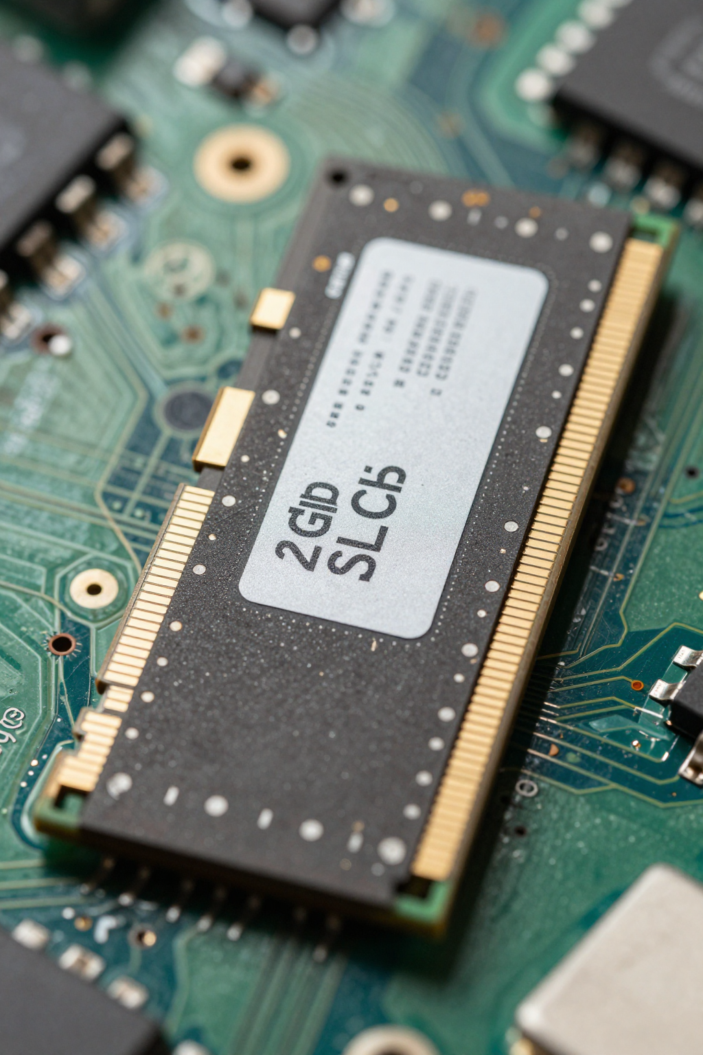
Quick Overview of Core Parameters for TC58NVG1S3HTA00
If you're holding a datasheet ready for design review, focusing on the core parameters in the following two dimensions will allow you to quickly determine whether this device meets your system requirements.
Storage Architecture and Capacity Specifications
TC58NVG1S3HTA00It adopts an SLC (Single-Level Cell) architecture, with a total capacity of 2 Gb, or 256 MB. Its page size is 2 KB plus a 64-byte spare area, and its block size is 128 KB, comprising 2,048 erasable blocks. The SLC architecture delivers a lifespan of 100,000 erase/write cycles and a lower bit error rate, which is especially critical for industrial control and network equipment applications requiring long-term stable operation. Compared to MLC or TLC, SLC's advantages in data retention and endurance make it the preferred choice for many engineers in the 2 Gb capacity range.
Electrical Characteristics and Interface Types
This device operates at a supply voltage of 3.3V (2.7V to 3.6V) and features an 8-bit parallel I/O interface, compatible with the standard NAND command set. Its page read time is 25 μs, page programming time is 200 μs, and block erase time is 2 ms. The interface speed supports standard timing in asynchronous mode, making it suitable for direct connection to low-cost controllers that do not require high-speed caching. Notably, its I/O pins are multiplexed for address, data, and command functions, which requires careful attention to bus loading and signal integrity during PCB layout.
Pin-by-pin breakdown of pin definitions
Pin definitions are the first step in verifying hardware compatibility.TC58NVG1S3HTA00It uses a 48-pin TSOP1 package; below is a functional grouping breakdown of key pins.
Detailed Explanation of Control Signal Pin Functions
Control signals include CLE (Command Latch Enable), ALE (Address Latch Enable), CE# (Chip Enable), RE# (Read Enable), WE# (Write Enable), WP# (Write Protect), and R/B# (Ready/Busy Output). The coordination between CLE and ALE determines the timing for latching commands and addresses; in terms of timing, they must be established and held before the rising edge of WE#. When WP# is low, programming and erasing are disabled; it is recommended to pull it low during the power-up initialization phase to protect data. R/B# is an open-drain output that requires an external pull-up resistor; its state directly indicates whether internal operations have completed, making it a key signal for polling at the driver layer.
I/O Bus and Power Pin Layout
I/O0 to I/O7 form an 8-bit bidirectional data bus, multiplexed for transmitting commands, addresses, and data. Power pins are divided into VCC (3.3V) and VSS (ground). The datasheet recommends placing a 0.1μF decoupling capacitor near each power pin and minimizing the return path length. Since parallel buses are prone to crosstalk during high-speed transitions, it is recommended to keep I/O traces of equal length and avoid crossing split planes. Additionally, unused I/O pins should not be left floating; they must be handled according to the recommended method to prevent leakage current or false triggering.
Key Timing Parameters and Performance Limits
Memorizing timing parameters alone is not enough; the key is understanding their relationship with system design margins. The following two sub-items will help you translate the numbers in the datasheet into practical design constraints.
| Parameter Symbol | Description | Typical Value/Maximum Value | Design Considerations |
|---|---|---|---|
| tR | Page Read Access Time | 25 μs (Max) | The controller must wait at least this amount of time before sampling data. |
| tPROG | Page Programming Time | 200 μs (Max) | It affects write throughput; the polling interval should be set appropriately. |
| tBERS | Block Erase Time | 2 ms (Max) | Erase operations take a long time, so sufficient timeout thresholds should be reserved. |
| tWP | WE# Pulse Width | 12 ns (Min) | PCB trace delays can reduce margin; it is recommended to reserve a 30% margin. |
Interpretation of Key Read/Write Timing Metrics
In the page read timing, the maximum tR (read access time) is 25 μs, meaning that from issuing the read command to data becoming available, the controller must wait at least 25 μs before sampling. For page programming, tPROG has a maximum of 200 μs, and for block erase, tBERS has a maximum of 2 ms. These parameters determine the timeout settings and polling intervals at the driver layer. If your controller has a relatively slow interrupt response, it is recommended to set the timeout threshold to 1.5 to 2 times the datasheet's maximum value, to avoid misjudging the busy state.
Timing Margin and System Design Margin
Timing margin is reflected in setup and hold times. Taking the WE# pulse as an example, the datasheet specifies a minimum tWP of 12 ns, but actual PCB trace delays and controller output jitter can erode this margin. It is recommended to reserve more than 30% timing margin during design, especially when the bus load is heavy or multiple devices share the bus. If you use an FPGA with a direct connection, you must explicitly declare these timing requirements in the constraint file and verify them through static timing analysis.
Selection Pitfalls: Common Misconceptions vs. Alternative Solutions
Selection errors often stem not from misreading parameters, but from overlooking hidden differences in package types, pin definitions, and command sets. The following two verification points can help you avoid the most common pitfalls.
Pin-to-Pin Compatibility Verification Points
Many engineers assume that NAND chips of the same capacity can be replaced pin-for-pin, butTC58NVG1S3HTA00The 48-pin TSOP1 definition is not an industry-standard. Before replacement, you must verify pin-by-pin that the positions of CLE, ALE, CE#, RE#, and WE# are consistent, paying particular attention to whether the R/B# pin is in the same location. Additionally, the size of the spare area and the OOB layout may vary among different manufacturers; if your file system relies on a specific OOB format, you will need to re-verify the bad block management logic after replacement. It is recommended to create a pin mapping table and check each candidate device item by item.
Domestic Substitution and Cost-Reduction Selection Strategy
Under cost-reduction pressure, domestically produced 2Gb SLC NAND is a common alternative. When selecting components, prioritize confirming three key points: whether the command set is compatible with standard NAND instructions, whether timing parameters fall within the original design margins, and whether the package and pin definitions allow for direct replacement. If pin-to-pin compatibility cannot be achieved, evaluate the cost of board redesign and the verification cycle. For projects already in mass production, it is recommended to first conduct small-batch trial production and run full read/write/erase cycle tests before deciding whether to switch. Cost reduction should not come at the expense of reliability, especially within industrial-grade temperature ranges.
Key Summary
- TC58NVG1S3HTA00This is a 2Gb SLC NAND with a page size of 2KB+64B, a block size of 128KB, and an endurance of 100,000 program/erase cycles.
- The pin definitions center around CLE, ALE, CE#, RE#, WE#, WP#, and R/B#. I/O0–I/O7 are multiplexed for commands, addresses, and data.
- Key timing parameters include tR 25μs, tPROG 200μs, and tBERS 2ms; a margin of at least 30% should be reserved during design.
- When selecting components, the key to avoiding pitfalls lies in pin-by-pin verification and a complete validation process for domestic replacements.
Frequently Asked Questions
TC58NVG1S3HTA00How is the 2Gb NAND capacity calculated?
2Gb means 2 gigabits, which divided by 8 equals 256MB. Internally, it is organized into 2,048 blocks, each 128KB, totaling 256MB. The actual usable capacity must account for bad blocks and file system overhead, typically estimated at 90% to 95% of the nominal capacity.
In the pin definitions, why does the R/B# signal require a pull-up resistor?
R/B# is an open-drain output; internally, the device can only pull low but cannot actively pull high. If no external pull-up resistor is connected, the signal state will be indeterminate when the bus is idle, potentially causing the controller to misinterpret whether the device is busy or free. It is recommended to connect a 4.7kΩ to 10kΩ pull-up resistor to VCC and ensure the pull-up resistor is placed close to the device.
When selecting a 2Gb NAND, how do you determine if the timing margins are sufficient?
Compare the maximum timing values in the datasheet with your controller's timeout settings, ensuring that the timeout threshold exceeds the maximum value. At the same time, calculate the PCB trace delay and the controller's output jitter, leaving a margin of at least 30%. If sharing the bus, also account for additional delays caused by multiple device loads.
TC58NVG1S3HTA00Can I directly replace it with another brand's NAND of the same capacity?
Do not assume a direct replacement. You must verify the definition of each pin on the 48-pin TSOP1, confirm that the control signals match the I/O locations, and ensure compatibility between the command set and the OOB layout. It is recommended to first create a pin mapping table, then conduct small-batch trial production to validate the entire read/write/erase process. Only after confirming everything is correct should you proceed with a full-scale transition.
