
Helping you deeply understand the 1Gb SLC NAND Flash chip, overcome signal integrity challenges, and ensure stable operation of storage systems.
When you receive the datasheet for the TC58NVG1S3ETA00, a 1Gb SLC NAND Flash chip, and face 48 pins and complex timing diagrams, do you feel lost? Unclear understanding of pin definitions directly leads to signal integrity issues in PCB design, read/write errors, and even chip damage. This article will provide a complete guide from pin function breakdown to practical PCB layout, helping engineers avoid common design traps and ensure storage system stability and reliability.
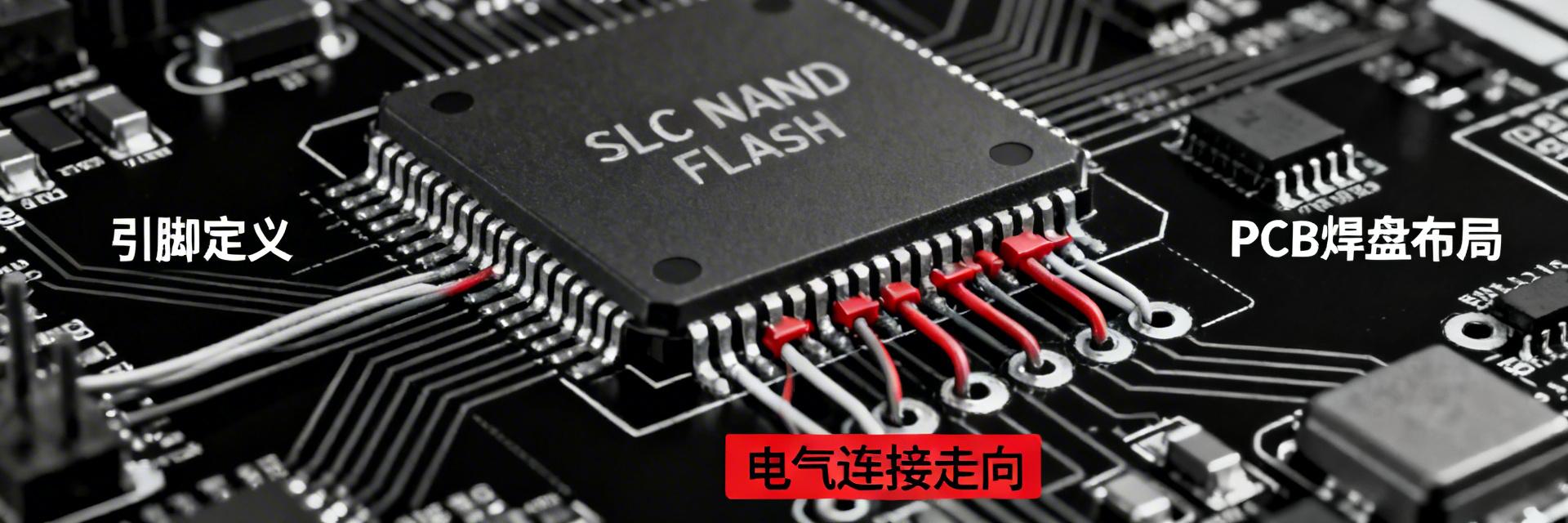
Chip Overview and Core Pin Function Analysis
The TC58NVG1S3ETA00 is a 1Gb SLC NAND flash memory in a TSOP-48 package. It is widely used in industrial control, network communications, and embedded storage due to its high reliability and relatively simple interface. Deeply understanding its pin functions is the first step to a successful design.
Core Power Supply Specifications (VCC/VCCQ)
Power and Ground Pins: The Foundation of Stable Operation
Power integrity is the basis of chip operation. The TC58NVG1S3ETA00 usually requires two sets of power supplies: VCC for core logic circuits and VCCQ specifically for I/O interface circuits. Multiple VSS (ground) pins must all be properly connected to the PCB ground plane to provide a low-impedance return path and suppress noise. In design, ensure a 0.1μF ceramic decoupling capacitor is placed near each pair of power and ground pins, as close to the pins as possible.
Control Signal Pins: In-depth Interpretation of CLE, ALE, CE#, RE#, WE#
Control pins act as the conductor's baton for the "dialogue" between the microcontroller and the flash memory chip. CLE (Command Latch Enable) and ALE (Address Latch Enable) signals determine whether commands or addresses are transmitted on the I/O lines. CE# (Chip Enable) is used to select the target chip, which is crucial in systems with multiple NAND chips in parallel. RE# (Read Enable) and WE# (Write Enable) control the timing of data reading and writing, respectively. These signals usually require pull-up resistors and should be routed as critical signal lines to ensure accurate timing.
Key Interface Signals and Timing Analysis
The reliability of data interaction directly depends on the quality of interface signals and strict adherence to timing. Any deviation can lead to initialization failure or data errors.
Data Input/Output Pins: I/Ox Multiplexing Mechanism and Pull-up/down Configuration
The I/O0-I/O7 pins of the TC58NVG1S3ETA00 are multiplexed, used to transmit commands, addresses, and data. This design saves pins but places higher demands on timing control. According to datasheet recommendations, these I/O lines usually require external pull-up resistors (e.g., 10kΩ) to ensure they are in a known high state when the bus is idle, avoiding false triggering. During PCB layout, these signal lines should be kept at equal lengths to reduce signal skew.
Read/Write Enable Timing: Setup/Hold Time Requirements and PCB Routing Impact
The datasheet explicitly specifies the setup time (tDS) and hold time (tDH) of the WE# and RE# signals relative to the data signals. For example, at a certain operating frequency, tDS may require at least 10ns. Delays introduced by PCB traces must be considered. Overly long traces or too many vias will increase signal propagation delay, potentially violating timing requirements and leading to sampling errors. Therefore, control signal lines should be as short and straight as possible and kept away from high-frequency noise sources.
Practical Guide to PCB Layout and Routing Pitfalls
Power Integrity Design
In addition to placing decoupling capacitors near the chip pins, power traces should be as wide as possible to reduce DC impedance. If using a multi-layer board, it is recommended to allocate independent power layers for VCC and VCCQ, or perform appropriate splitting. Ensure the power network is clean to avoid digital noise from coupling into the chip's core circuitry through the power supply.
Signal Integrity Design
Control signals (such as CLE, ALE, WE#, RE#) should be treated as a group, with trace lengths matching as closely as possible. The data bus I/O[7:0] should also be routed with equal lengths as a group. All signal lines should reference a complete ground plane, avoiding crossing power supply split gaps to prevent electromagnetic interference from discontinuous return paths.
Key Summary
- ● Power and Ground are Fundamental: Ensure VCC, VCCQ, and all VSS pins are solidly connected, and high-quality decoupling capacitors are placed adjacent to the pins. This is the primary condition for the stable operation of the TC58NVG1S3ETA00.
- ● Control Timing is Key: Strictly follow the setup and hold times for control signals such as CLE, ALE, WE#, and RE#. During PCB layout, prioritize shortening these critical path trace lengths to avoid timing risks.
- ● PCB Layout Determines Success: Adopting strategies such as power plane splitting, signal group equal-length routing, and maintaining a complete ground plane reference can greatly enhance signal integrity and guarantee data transmission accuracy.
- ● Reserve Debugging Interfaces: Reserving test points for key signals during the PCB design phase provides great convenience for subsequent production testing and troubleshooting.
Frequently Asked Questions (FAQ)
Why might the TC58NVG1S3ETA00 fail to be recognized by the controller after power-up? +
How to troubleshoot random data errors when reading or writing to the TC58NVG1S3ETA00? +
What suggestions are there for improving mass production reliability when using the TC58NVG1S3ETA00 in a design? +
Technical Verified Layout Design
