
As the demand for high reliability and small-footprint storage in embedded systems continues to grow, requirements for storage chips in industrial control and the Internet of Things (IoT) have expanded beyond mere capacity. When faced with lengthy datasheets, engineers often feel overwhelmed during the design process. The TC58BVG0S3HBAI6, a classic model in the Toshiba/Kioxia NAND Flash family, has been widely adopted in fields like industrial control and smart homes due to its outstanding stability. But do you truly understand its most critical parameters? This guide dives into the core of the datasheet to help you quickly grasp the 5 key parameters that determine system stability, compatibility, and cost, enabling precise selection.
1. TC58BVG0S3HBAI6 Overview and Market Positioning
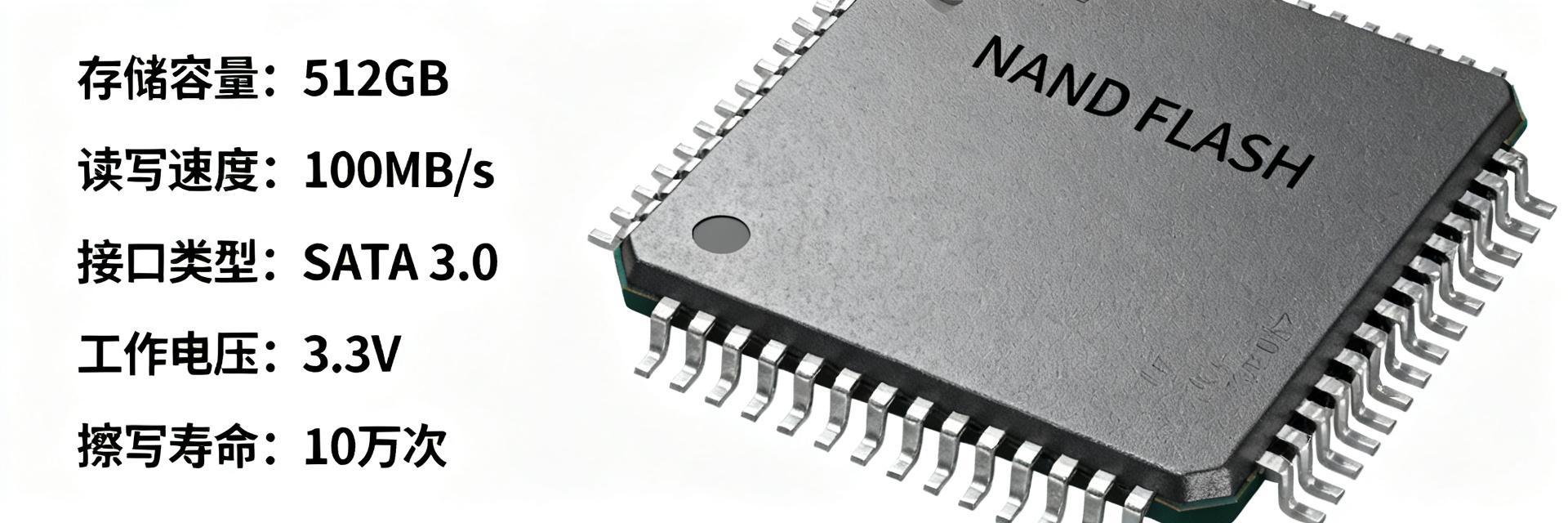
Before diving into the parameters, it is essential to understand the market positioning of this chip. It is not a product pursuing extreme capacity, but rather one that prioritizes "reliability," playing an irreplaceable role in specific sectors.
Core Architecture: The Persistence and Advantages of SLC NAND Flash
The TC58BVG0S3HBAI6 is a 1Gbit (128MB) SLC NAND Flash. Compared to mainstream MLC or TLC NAND Flash, SLC (Single-Level Cell) offers significant advantages in read/write speed, endurance (P/E cycles), and data retention. The datasheet parameters clearly demonstrate this: its typical P/E cycle life far exceeds that of MLC/TLC, and data can be retained for up to 10 years even in high-temperature environments of 85°C. This "slow and steady" characteristic makes it the preferred choice for designers in applications with extremely high data integrity requirements, such as industrial control and automotive electronics.
Key Application Scenarios: From Industrial Control to Smart Homes
You might wonder where this chip is specifically used. Its application scenarios are broad, ranging from complex industrial equipment to simple smart terminals. Common applications include: industrial control devices like PLCs (Programmable Logic Controllers), boot disks for embedded Linux systems, smart meters, and On-Board Diagnostic (OBD) systems. Furthermore, its wide operating temperature range (-40°C to +85°C) and excellent vibration resistance allow it to operate stably in harsh environments, such as factory floors or high-speed vehicles.
2. Deep Decoding of the 5 Core Parameters
Now, let's get straight to the point and decode the 5 most critical parameters in the datasheet. Understanding these parameters is key to your successful application of the TC58BVG0S3HBAI6.
Parameter 1: Storage Capacity and Page/Block Structure
First, let's interpret the meaning of "1Gbit (128M x 8bit)." The total capacity is 1Gbit, which translates to 128MB. More importantly, its organization: a Page is 2KB, and a Block consists of 64 pages, totaling 128KB. This structure directly affects your data read/write and erase strategies. For instance, to modify part of the data on a page, you must first read the entire block (128KB) into a buffer, modify it, erase the entire block, and then write the data back.
Parameter 2: Read/Write Interface Timing and Speed
This is core to evaluating system performance bottlenecks. The datasheet defines several key timing parameters, such as tRC (Read Cycle Time) and tWC (Write Cycle Time), typically around 25ns; as well as tPROG (Page Program Time, typical 200μs) and tBERS (Block Erase Time, typical 2ms). By calculation, its theoretical throughput can be derived: read speed is close to 40MB/s, and write speed is approximately 10MB/s. When designing drivers, ensure you configure hardware or software state machines based on these timing parameters.
Parameter 3: Power Management and Consumption Performance
For battery-powered devices, power consumption is vital. The TC58BVG0S3HBAI6 operates within a voltage range of 2.7V to 3.6V, compatible with most 3.3V systems. The datasheet lists operating currents for different modes: ~15mA during read, ~20mA during programming, and ~10mA during erase. Most noteworthy is its standby current (< 50μA) and ultra-low power consumption in sleep mode (< 10μA).
Parameter 4: Reliability Indicators (Endurance and Error Correction)
The TC58BVG0S3HBAI6 datasheet promises a P/E (Program/Erase) cycle life of up to 100,000 cycles and 10-year data retention at 85°C. The manual recommends at least 1-bit/512-byte error correction capability. In actual designs, using a 4-bit or 8-bit hardware BCH ECC engine can further extend the chip's usable life.
Parameter 5: Package and Pin Functions
This chip primarily uses the TSOP-48 package. You need to understand the functions of core pins, such as CLE, ALE, CE, RE, WE, and the I/O multiplexed data lines. During PCB layout, pay special attention to placing VCC and VSS filtering capacitors close to the chip pins to reduce power noise. It is recommended to keep I/O line lengths equal to avoid signal timing skew.
3. Selection Guide Based on Core Parameters
Having understood the parameters above, the next step is how to apply them for precise selection. This requires combining the parameters with specific project needs.
Selection Step 1: Precise Matching of Capacity and Performance
First, determine if the 128MB capacity is sufficient based on your firmware size, log storage space, and data caching requirements. For example, a simple IoT sensor node might only need 32MB for firmware and 64MB for logs, making the 128MB capacity of the TC58BVG0S3HBAI6 more than enough. Second, evaluate if its 10MB/s write speed meets your requirements based on your data throughput needs.
Selection Step 2: Confirmation of Power and I/O Interface Compatibility
This is the most error-prone step. The I/O voltage of your host controller must match the operating voltage range (2.7V to 3.6V) of the TC58BVG0S3HBAI6. If your system uses 1.8V logic while the chip is 3.3V, level shifting is required. Voltage mismatch can lead to the chip failing to operate or even permanent damage.
Selection Step 3: Considering Long-term Supply and Cost Balance
It is recommended to confirm the Product Longevity Program (PLP) with the manufacturer or distributor after prototype validation. Regarding cost, while the unit price of SLC NAND Flash is higher than MLC/TLC, its Total Cost of Ownership (TCO) is often lower when considering the resulting system reliability improvements (reduced after-sales maintenance costs).
Key Summary
- Understand SLC Architectural Advantages: The SLC architecture of the TC58BVG0S3HBAI6 determines its irreplaceable reliability in industrial control, serving as the foundation for selection.
- Decode Core Parameters: Mastering capacity structure, R/W timing, power consumption, reliability, and packaging is key to reading the datasheet and evaluating system performance.
- Precisely Match System Requirements: During selection, cross-check the above parameters against your system's capacity, performance, power, and reliability requirements.
Frequently Asked Questions (FAQ)
Does the TC58BVG0S3HBAI6 require external ECC?
Yes. Although SLC has lower ECC requirements than MLC/TLC, the datasheet still recommends at least 1-bit/512-byte error correction capability. In actual industrial-grade designs, using 4-bit or 8-bit hardware BCH ECC engines is typically recommended to ensure data integrity.
How to confirm if the power supply design for TC58BVG0S3HBAI6 is reasonable?
You need to ensure that the 3.3V voltage ripple provided by your power chip is sufficiently small (typically less than 100mV). Additionally, place 0.1μF and 10μF decoupling capacitors near the VCC and VSS pins, keeping the traces as short and thick as possible.
What is the initialization process for TC58BVG0S3HBAI6?
The basic initialization flow is: after power-up, wait for the chip to stabilize (typically 1ms), then send the Reset command (FFh) and wait for the internal reset to complete. Next, verify if the chip is normal by sending the Read ID command (90h). Finally, configure relevant functions as needed.
