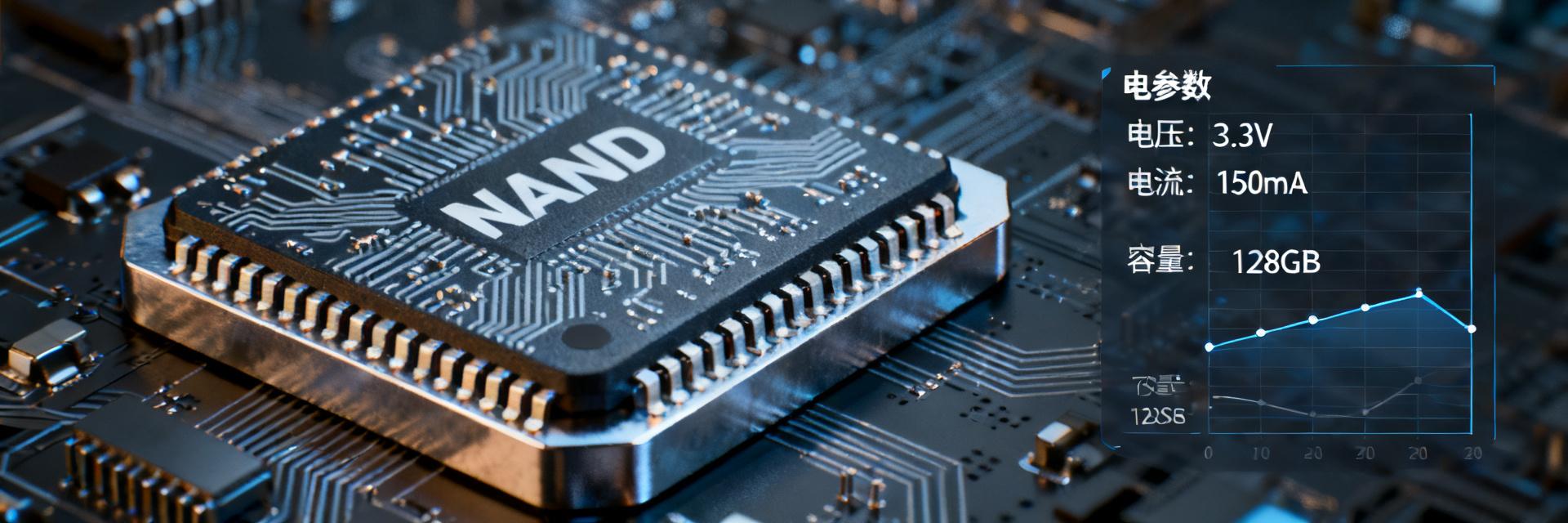
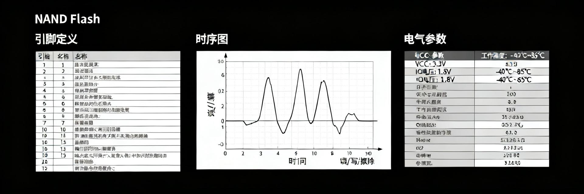
在工业控制、通信基站和汽车电子等严苛领域,TC58BVG2S0HBAI4 作为 KIOXIA(原东芝存储)出品的经典 4Gb SLC NAND Flash,凭借其卓越的耐久性成为高可靠性方案的首选。本文基于官方 Data Sheet,为您拆解其核心技术规格。 核心技术规格概览 特性参数 技术指标 应用优势 存储容量 4 Gbit (512M x 8-bit) 大容量固件存储 存储单元 SLC (Single Level Cell) 极高稳定度与寿命 擦写次数 (P/E) 100,000 Cycles 支持频繁数据写入 工作电压 2.7V to 3.6V (Single) 兼容主流工业电源 TC58BVG2S0HBAI4 (SLC) CE# / WE# ALE / CLE I/O [0:7] VCC / GND 核心架构解析:512M x 8-bit 的精密组织 TC58BVG2S0HBAI4 的存储架构由 2,048 个块(Blocks)组成,每个块包含 64 个页(Pages)。每页具备 (4K + 256) 字节的容量。这种大页面(Large Page)架构在执行顺序读写时具有极高的效率。作为 SLC 芯片,其每个单元仅存储 1 比特,这使得它在恶劣电磁环境下依然能保持极低的误码率(BER)。 电参数与信号完整性设计 DC 特性:功耗控制的关键 该芯片的读操作电流典型值为 25mA,待机电流仅 50μA。对于手持式工业设备,这种低待机功耗能显著延长电池寿命。设计时需在 VCC 引脚配置 0.1μF + 10μF 的并联退耦电容,以平滑由于高频擦写操作引起的瞬态电流波动。 AC 特性:时序约束红线 tRC (Read Cycle Time): 25ns (Min),确保高速连续读取性能。 tPROG (Page Program Time): 300μs (Typ),提供均衡的写入吞吐量。 tBERS (Block Erase Time): 3ms (Typ),快速回收存储空间。 封装与可靠性管理:TSOP I 48-Pin TSOP I 封装提供了成熟的焊接工艺兼容性。由于 SLC NAND 在物理上仍存在极小概率的比特翻转,工程师在固件层必须实现 ECC (Error Correction Code)。推荐算法为 1-bit ECC/528 bytes。此外,系统必须包含 坏块管理逻辑 (Bad Block Management),在初始化时通过扫描 Spare Area 的标记来建立映射表。 常见问题解答 (FAQ) TC58BVG2S0HBAI4的典型擦写次数是多少? 作为高性能 SLC NAND Flash,TC58BVG2S0HBAI4 的典型擦写寿命达到 100,000 次(P/E Cycles),远超 MLC 或 TLC 架构,适合频繁更新的高频应用场景。 TC58BVG2S0HBAI4的数据保持能力如何? 在 -40°C 至 85°C 的宽温工作环境下,该芯片提供长达 10 年的数据保持能力。这使其成为工业设备存放关键 OS 镜像和引导程序的理想选择。 TC58BVG2S0HBAI4需要外部ECC吗? 强烈建议使用。虽然 SLC 极度稳定,但为了应对长期运行中宇宙射线或电荷流失导致的比特翻转,建议在主控端实现至少 1-bit ECC 纠错。 TC58BVG2S0HBAI4的封装尺寸是多少? 该芯片采用标准的 48-pin TSOP I 封装,物理尺寸为 18.4mm x 12.0mm x 1.2mm,引脚间距(Pitch)为 0.5mm,适合高密度 SMT 贴片工艺。
2026-07-02 10:40:13
When you receive a brand-new TC58BVG1S3HTA00 2Gb NAND Flash chip, facing the dense pin definitions and complex timing diagrams, you often need to quickly extract key information to avoid design pitfalls. This article provides a clear datasheet interpretation guide to ensure your project succeeds from schematic design to code implementation. Core Overview and In-depth Pin Function Analysis TC58BVG1S3HTA00 is a 2Gb (256MB) SLC NAND Flash produced by KIOXIA, featuring 3.3V power supply and a standard TSOP-48 package. During PCB layout, be sure to note the orientation mark for Pin 1 to avoid soldering errors. I/O0-7 CLE ALE VCC R/B# GND TSOP-48 Key Signal Logical Grouping Pin Name Functional Description Design Points CLE / ALE Command/Address Latch Enable Distinguishes the data type on the bus; must strictly meet setup times tCLS/tALS. R/B# Ready/Busy Signal Open-drain output; must have an external 4.7kΩ~10kΩ pull-up resistor. I/O0 - I/O7 8-bit Bidirectional Data Bus Transfers commands, addresses, and data; traces should be equal length to reduce skew. CE# / WE# / RE# Chip/Write/Read Enable Signals Core for controlling operation timing; pay attention to signal reflection at high frequencies. Read/Write Timing and Performance Parameters Understanding the timing of TC58BVG1S3HTA00 is the foundation for writing drivers. All operations are triggered by the edges of WE# or RE#; below are key timing parameters that must be referenced in system design. Core Timing Parameters (AC Characteristics) tR (Page Read Time): Typical value 25µs. This is the time from sending a read command until data is ready in the cache. tPROG (Page Program Time): Typical value 200µs. The average time taken to write one page. tBERS (Block Erase Time): Typical value 1.5ms. The time to erase one block; system scheduling needs to reserve this delay. tRC / tWC (Read/Write Cycle): Minimum 25ns. Determines the maximum frequency of data transfer. Hardware Design and PCB Layout Recommendations To ensure the stability of 2Gb large-capacity storage, power design and signal integrity are critical: Power Filtering: Place a 0.1µF ceramic capacitor close to the VCC pin, and add a 4.7µF tantalum capacitor to handle burst currents (approx. 30mA) during programming. Impedance Control: It is recommended to control I/O bus length differences within 500mil, and signal lines should stay away from switching power supply areas. Power-on Reset: Wait 100µs after VCC stabilizes, then send the FFh reset command and confirm communication by reading the 90h ID. Frequently Asked Questions (FAQ) What is the VCC supply voltage range for TC58BVG1S3HTA00? The standard operating voltage is 3.3V, and the allowable voltage range is typically between 2.7V and 3.6V. The design should ensure the regulator output is stable to avoid transient voltage drops below 2.7V. How to handle bad blocks in TC58BVG1S3HTA00? NAND Flash may have bad blocks from the factory. System software must scan the entire disk and establish a Bad Block Management Table (BBT) before first use. Except for the first 1-2 blocks guaranteed to be usable, other areas must have their Status Register checked after operation. Why must the R/B# pin be connected to a pull-up resistor? R/B# is an open-drain output, which can only pull the signal low. If no pull-up resistor is connected, the pin will be in a floating state when the chip is in the Ready state, preventing the MCU from recognizing the high level. What is the standard code flow for power-on initialization? 1. Wait for VCC to stabilize; 2. Delay 100µs; 3. Send Reset command (FFh); 4. Monitor R/B# turning high; 5. Send Read ID command (90h) to verify chip identity.
2026-06-27 11:03:16